The AFM & Quantum Transport measurements are aimed at shedding light on some fundamental questions about electrical transport in two-dimensional electron gasses/1D nanowires/graphene. Our current research focuses on studying local electronic properties of 2D van der Waals materials such as MoS2, WSe2, graphene and various topological insulators.
Imaging Andreev Reflection in Graphene
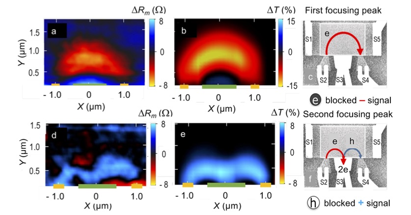
Shown below is an image of Andreev reflection in graphene obtained using the cooled scanning gate microscope. Fig a shows an image of cyclotron orbit of electrons at first magnetic focusing peak while Fig c shows an image of Andreev reflection. Fig b and d are the simulations for cyclotron orbits of electrons and Andreev Reflection respectively.
Electron Flow through collimating contacts in Graphene
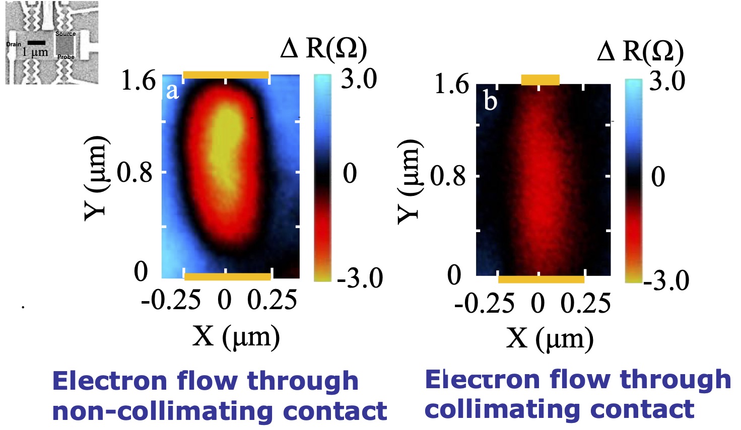
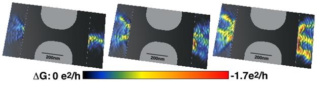
Shown below is an image of electron flow through collimating contacts in graphene obtained using the cooled scanning gate microscope. Fig a shows an image when the collimating contact is turned off and Fig b shows the electron flow when collimating contact is turned on.
Cyclotron orbit of electrons in Graphene
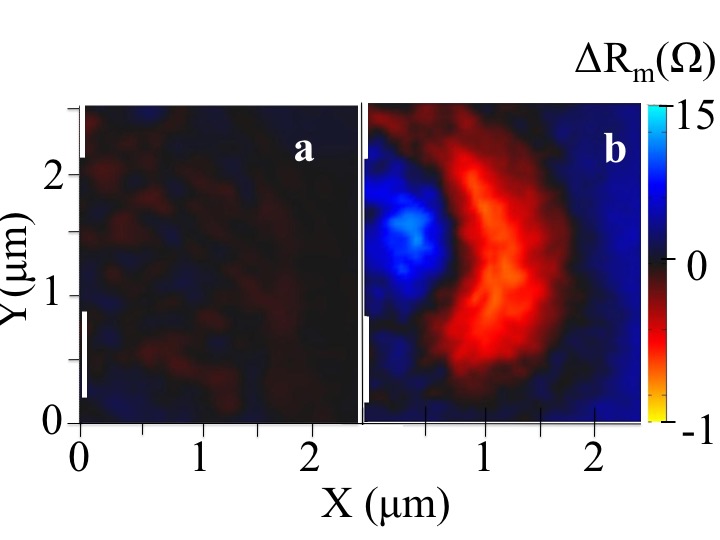
Shown below is an image of cyclotron orbits in graphene obtained using the cooled scanning gate microscope. Fig a shows an image when the magnetic field is turned off and Fig b shows the cyclotron orbit when magnetic field is on.
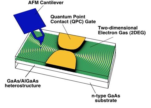
Two Dimensional Electron Gas
Shown below is a sketch illustrating the basic idea behind these experiments:
The term "two dimensional electron gas" (2DEG) refers to the thin sheet of highly mobile conduction electrons which forms
just beneath the surface of specially grown wafers. In this lab we use GaAs/AlGaAs heterostructures with 2DEGs located approximately
50nm beneath the surface. The combination of extremely long mean free path and long coherence times found in these systems at low
temperature presents a unique opportunity to study coherent, ballistic electron flow through nano-scale devices.
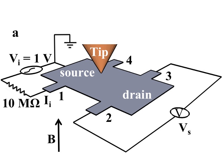
The picture above illustrates one way that the AFM can be used to probe the transport through a typical 2DEG device, in this case a
point contact. By simultaneously scanning the negatively charged AFM tip over the surface and measuring the conductance, (or other
electrical characteristics) of the sample, one can image the current flow in the 2DEG. The negative charge on the cantilever tip causes
electrons in the 2DEG immediately underneath the tip to be "pushed away", causing a local depletion region directly below the
tip. Electrons flowing in the 2DEG are backscattered by this depletion region back through the Quantum Point Contact (QPC) reducing the
conductance. When the tip moves over regions of high electron flow there is a large change in the conductance. When the tip is over
regions of relatively low electron flow, there is no chance in conductance. By scanning the tip over the sample, and simulatenously
measuring the change in conductance, the two-dimensional current density in a device is imaged.
The picture below shows the electron flow from the first three modes of a QPC. Moving from left to right the QPC is opened from the 1st to the 2nd and then the 3rd mode. As each new mode is added new branches of current appear. Also, the images are decorated by interference fringes spaced by half the Fermi wavelength. These are due to constructive and deconstructive backscattering of electron waves from the tip back through the QPC. They demonstrate that we are imaging coherent electron wave flow.
For 2DEG devices larger than both the mean free path and the phase coherence length, electron transport is well described by classical, diffusive models. Current commercial semiconductor devices are usually in this limit.For smaller electronic devices, however, quantum mechanics plays an increasingly dominant role. This regime, often referred to as mesoscopic physics, (between microscopic and macroscopic), has been an area of active research for the past decade or so, and a wide variety of novel, interesting physical phenomena have been discovered and investigated. These include the Quantum Hall Effect, Quantum Chaos, Tunable Point Contacts (with resulting Conductance Quantization), and Quantum Dots (which illustrate Coulumb Blockade). Throughout all of these experiments, however, the actual charge and current distributionis only indirectly measurable. We are interested in directly spatially imaging the charge and current flow through devices like these.
Imaging cyclotron orbits in graphene
Graphene is an exciting new material with properties that are radically different from traditional semiconductors. We use our home-built liquid-He-cooled scanning probe microscope (SPM) to probe the motion of electrons in graphene. The SPM tip can be used to create a change in the density of electrons locally.
Using atomically flat hexagonal boron nitride as substrates, ballistic motion of electrons can be achieved in graphene. Electrons follow cyclotron trajectories when a magnetic field is applied normal to the graphene plane. For a Hall bar geometry sample, the magnetic field focuses a current Ii, injected from one lead into another lead located an integer number of cyclotron diameters away creating a voltage, Vc. The degree of focusing is measured in the transresistance, Rm= Vc/Ii. We use a cooled scanning gate microscope to image such cyclotron trajectories in graphene.
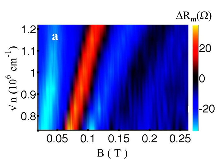
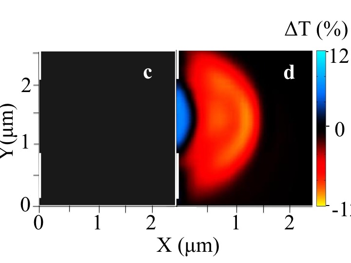
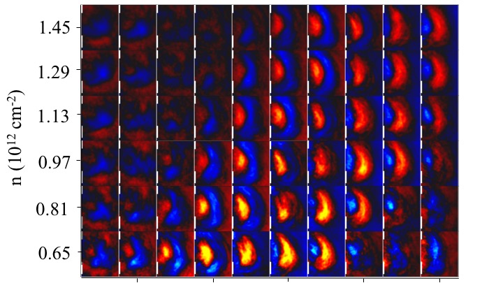
The sample is a high mobility hBN-graphene-hBN sandwich etched into hall bar geometry. By tuning the transverse magnetic field B and density n in the graphene layer, we can observe the first few magnetic focusing peaks (above figure). For values of B and n on first magnetic focusing peak in the above figure, we observe an image of the cyclotron orbit that extends from one lead to the other as shown below in figure b and d. Fig. b and d are the experimental and simulated images of cyclotron orbits of electrons in graphene. Fig. a and c show the images at zero applied magnetic field for experiment and simulation respectively.
We also study the effects of B and n on the spatial distribution of electron trajectories. A tiled plot of all the images obtained with B and n dependence is as shown below.
One dimensional systems
Nanowire heterostructures define high-quality few-electron quantum dots for nanoelectronics, spintronics,and quantum information processing. We use a cooled scanning probe microscope (SPM) to image and control an InAs quantum dot in an InAs/InP nanowire using the tip as a movable gate. Images of dot conductance vs tip position at T=4.2 K show concentric rings as electrons are added, starting with the first electron.
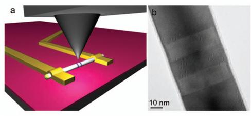
The above image shows the schematic of the scanning gate microscopy on a nanowire. Conductance between source and drain electrodes is recorded vs tip position to obtain an image. The right image is TEM image of an InAs/ InP heterostructure nanowire
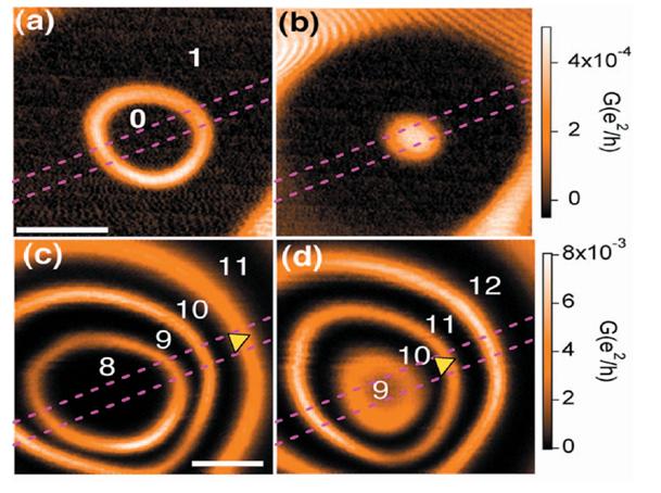
SPM Coulomb-blockade conductance images (a) and (b) of the last electron on the InAs nanowire quantum dot and (c) and (d) of a higher number of electrons vs tip position as the tip is scanned in a plane 100 nm above the dot. The dotted lines show the location of the nanowire. The rings of high conductance correspond to Coulomb-blockade conductance peaks. The integers indicate the number of electrons on the dot when the tip lies inside or between the rings.
Universal Conductance Fluctuations in Graphene
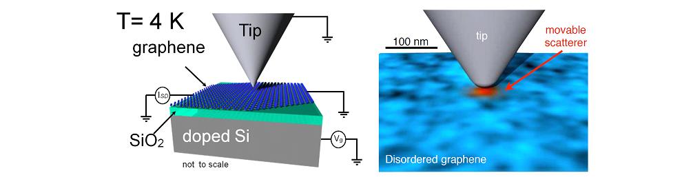
Schematic diagram of the charged scanning probe microscope tip creating an additional scatterer (red) in graphene. The shaded blue color scale in the graphene layer represents the disorder potential.
At low temperatures, the coherent interference of electron waves scattered by disorder leads to quantum effects such as universal conductance fluctuations (UCF) and weak localizations. Using the SPM tip as a movable scatterer, these conductance fluctuations are mapped vs. the tip position. For UCF we find conductance images that resemble speckle patterns, that change by δG ~ e^2/h when the tip moves by half the Fermi wavelength.
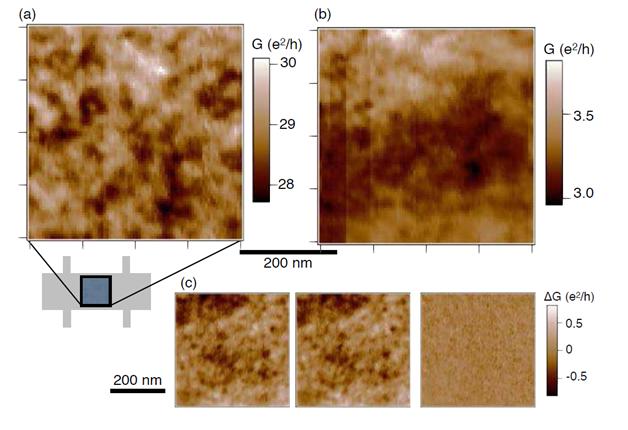
Conductance images (a) far from the dirac point and (b) near the dirac point. Figure (c) shous the repeatability of the conductance images showing the difference between the first two images. Our conductance images also probe coherent scattering and weak localization in magnetic fields.
|
 Westervelt Group 2016 | webmaster: Sagar Bhandari Westervelt Group 2016 | webmaster: Sagar Bhandari
|
|